


Effect of Film Thickness on Mechanical Properties of Si-based SiO2 Thin Films
-
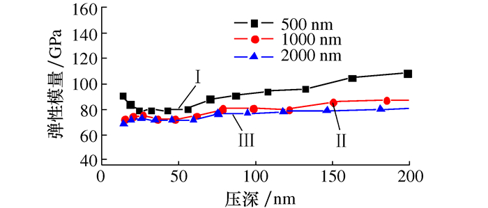
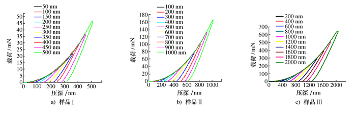
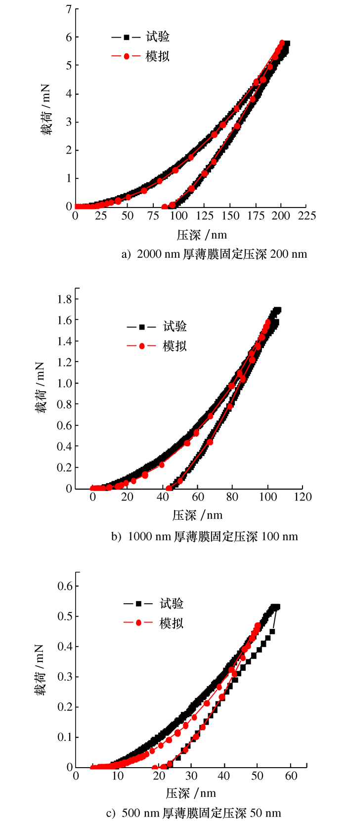
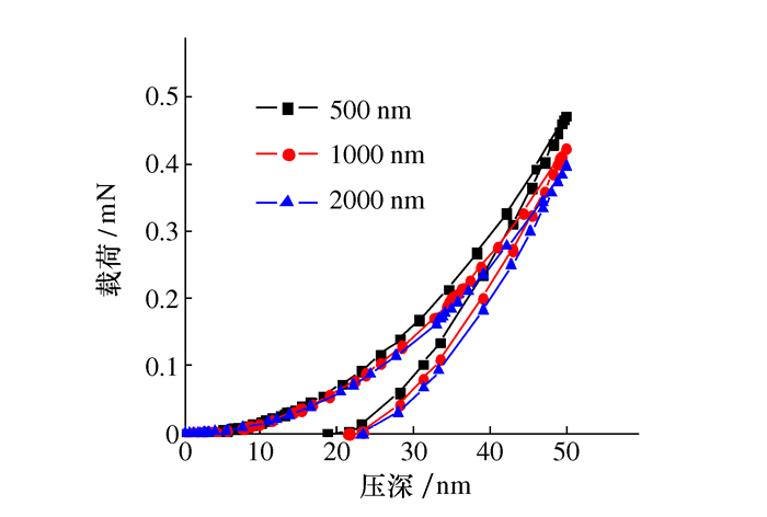
摘要: 为了研究薄膜厚度对Si基SiO2薄膜力学性能的影响规律,利用纳米压痕技术及有限元模拟方法对不同厚度的Si基SiO2薄膜材料进行测试,分析了不同厚度薄膜的硬度及弹性模量等力学性能,讨论了不同压深膜厚比对不同厚度薄膜弹性恢复率的影响,并在试验的基础上,建立了有限元模型,模拟了不同厚度薄膜在相同压深下的载荷位移关系,分析了薄膜的弹性恢复性能。结果表明:SiO2薄膜越厚其弹性模量越小,而薄膜的硬度在薄膜较薄时压痕的尺寸效应更明显,并利用模拟进一步分析得出薄膜越薄弹性恢复性能越好。Abstract: In order to study the effect of the film thickness on the mechanical properties of Si-based SiO2 films, nanoindentation technology and finite element simulation of ABAQUS were used to test Si-based SiO2 films with different thicknesses. The mechanical properties including the hardness and elastic modulus of films with different thicknesses were analyzed. The effects of the pressure depths and film thickness ratios on the elastic recovery rate of films with different thicknesses are discussed. Based on the experiments, the finite element model was established. The load-displacement relationship of films with different thickness under the same pressure depth was simulated, and the elastic recovery performance of the film was analyzed. The results show that the thicker the SiO2 film is, the smaller the elastic modulus is. When the film is thin, the size effect of the indentation of the film is more obvious, and further analysis by using simulation shows that the thinner the film is, the better the elastic recovery performance is.
-
Key words:
- Si-based SiO2 thin films /
- nanoindentation /
- FEM /
- elastic modulus /
- hardness
-
表 1 模拟材料参数
名称 弹性
模量/GPa泊松比 屈服
强度/GPa切线
模量/GPaSiO2薄膜 81 0.27 7.15 8.45 Si基底 180 0.23 9.14 10.98  下载: 导出CSV
表 2 不同厚度SiO2薄膜塑性参数
参数名称 500 nm 1000 nm 2000 nm 弹性模量/GPa 88 81 77 屈服强度/GPa 8.7 7.15 6.3 切线模量/GPa 9.45 8.45 8.35
下载: 导出CSV
-
[1] Liu G Y, Ni S, Song M. Effect of indentation size and grain/sub-grain size on microhardness of high purity tungsten[J]. Transactions of Nonferrous Metals Society of China, 2015, 25(10):3240-3246 doi: 10.1016/S1003-6326(15)63958-9 [2] 孙俊峰, 石霞.PECVD SiO2薄膜内应力研究[J].半导体技术, 2008, 33(5):397-400 doi: 10.3969/j.issn.1003-353X.2008.05.009Sun J F, Shi X. Study of internal stress in PECVD SiO2 thin films[J]. Semiconductor Technology, 2008, 33(5):397-400(in Chinese) doi: 10.3969/j.issn.1003-353X.2008.05.009 [3] 李默.硅微通道结构对SiO2薄膜热应力的影响[D].长春: 长春理工大学, 2013Li M. Effect of micro-channel structure on thermal stresses of silicon dioxide film[D]. Changchun: Changchun University of Science and Technology, 2013(in Chinese) [4] Liu H S, Wang L H, Jiang Y G, et al. Study on SiO2 thin film modified by post hot isostatic pressing[J]. Vacuum, 2018, 148:258-264 doi: 10.1016/j.vacuum.2017.11.018 [5] Rakshit S, Tripuraneni R, Nadimpalli S P V. Real-time stress measurement in SiO2 thin films during electrochemical lithiation/delithiation cycling[J]. Experimental Mechanics, 2018, 58(4):537-547 doi: 10.1007/s11340-017-0371-2 [6] Bhushan B. Nanotribology and nanomechanics[M]//Bhushan B. Springer Handbook of Nanotechnology. Berlin, Heidelberg: Springer, 2010: 1227-1265 [7] Liu S, Huang H, Gu Y T. Deconvolution of mechanical properties of thin films from nanoindentation measurement via finite element optimization[J]. Thin Solid Films, 2012, 526(1):183-190 http://www.wanfangdata.com.cn/details/detail.do?_type=perio&id=ec4d43b063cf8c8b10c8a078ead958c3 [8] Karimzadeh A, Ayatollahi M R, Alizadeh M. Finite element simulation of Nano-indentation experiment on aluminum 1100[J]. Computational Materials Science, 2014, 81:595-600 doi: 10.1016/j.commatsci.2013.09.019 [9] Shan Z H, Sitaraman S K. Elastic-plastic characterization of thin films using nanoindentation technique[J]. Thin Solid Films, 2003, 437(1-2):176-181 doi: 10.1016/S0040-6090(03)00663-1 [10] Chatterjee A, Kumar N, Abelson J R, et al. Nanoscratch and nanofriction behavior of hafnium diboride thin films[J]. Wear, 2008, 265(5-6):921-929 doi: 10.1016/j.wear.2008.02.002 [11] Yu C, Yang R, Feng Y H, et al. Relationships between the work recovery ratio of indentation and plastic parameters for instrumented spherical indentation[J]. MRS Communications, 2015, 5(1):89-94 doi: 10.1557/mrc.2015.10 [12] Kim M, Marimuthu K P, Lee J H, et al. Spherical indentation method to evaluate material properties of high-strength materials[J]. International Journal of Mechanical Sciences, 2016, 106:117-127 doi: 10.1016/j.ijmecsci.2015.12.008 [13] 张晓玲.薄膜厚度对其纳米压痕行为影响的有限元分析[D].哈尔滨: 哈尔滨工业大学, 2005Zhang X L. Finite element analysis of the influence of film thickness on the nanoindentation behavior[D]. Harbin: Harbin Institute of Technology, 2005(in Chinese) [14] 王海斗, 董美伶, 崔秀芳, 等.不同厚度纳米Ti薄膜的力学性能[J].材料工程, 2015, 43(11):50-56 doi: 10.11868/j.issn.1001-4381.2015.11.009Wang H D, Dong M L, Cui X F, et al. Mechanical properties of Nano Ti films with different thickness[J]. Journal of Materials Engineering, 2015, 43(11):50-56(in Chinese) doi: 10.11868/j.issn.1001-4381.2015.11.009 [15] 吴子景, 吴晓京, Shen W D, 等.集成电路钝化层薄膜的纳米力学性质研究[J].西安交通大学报, 2008, 42(11):1345-1349 http://d.old.wanfangdata.com.cn/Periodical/xajtdxxb200811007Wu Z J, Wu X J, Shen W D, et al. Nanomechanical properties of passivation thin films in integrated circuit[J]. Journal of Xi'an Jiaotong University, 2008, 42(11):1345-1349(in Chinese) http://d.old.wanfangdata.com.cn/Periodical/xajtdxxb200811007 [16] 陈秀.MEMS薄膜纳米压痕法测试和仿真研究[D].北京: 北京理工大学, 2014Chen X. Test and simulation of MEMS film based on Nano-indentation[D]. Beijing: Beijing Institute of Technology, 2014(in Chinese) [17] 王月敏, 闫相桥, 李垚, 等.基于纳米压痕技术的本构关系反演分析进展[J].材料导报, 2017, 31(17):1-5 doi: 10.11896/j.issn.1005-023X.2017.017.001Wang Y M, Yan X Q, Li Y, et al. A review of reverse analysis for material constitutive relation based on nanoindentation technique[J]. Materials Review, 2017, 31(17):1-5(in Chinese) doi: 10.11896/j.issn.1005-023X.2017.017.001 [18] Zhao M H, Chen X, Xiang Y, et al. Measuring elastoplastic properties of thin films on an elastic substrate using sharp indentation[J]. Acta Materialia, 2007, 55(18):6260-6274 doi: 10.1016/j.actamat.2007.07.045 -


 点击查看大图

图(7) / 表(2)
计量
- 文章访问数: 380
- HTML全文浏览量: 117
- PDF下载量: 50
- 被引次数: 0
